STMicroelectronics Used Moldex3D to Solve Void Issues During Chip Encapsulation Process
Among the world’s largest semiconductor companies, STMicroelectronics has 46,000 creators and makers of semiconductor technologies, devices, and solutions that start with their employees, 100,000 customers, and thousands of partners. (Source) STMicroelectronics engineers minimize the risk of incomplete resin filling by employing Moldex3D IC Packaging solution. First, the software allows to reproduce void formation caused by unbalanced flow behavior. Then, Moldex3D simulation is applied to optimized package design to reduce the risk of issues. As a result, geometric variations show a significant effect on filling front progression avoiding the generation of structural defects during the molding process. Virtual failure anticipation with Moldex3D is successful and results are transferred to package prototyping for new product integration. STMicroelectronics designers estimate a reduction of unbalanced resin flow between the top and the bottom of the cavity by decreasing the die pad size of the standard configuration. Since the lead frame die pad has been identified as a critical location, the optimization of its design shows significant benefits in terms of filling behavior. In fact, this approach reduces the presence of critical weld lines in the product. Therefore, this solution solves void issues acting first on design rather than experimental prototyping which requires time and money. IC encapsulation is the process of encapsulating microchips by injecting epoxy molding compound (EMC) into a mold cavity, and the plunger is used to press a tablet into the cavity like Fig. 1. Common problems in IC packaging are incomplete filling, internal voids, and wire sweeping and crossing showing in Fig. 2. To prevent production loss and customer complaint, these issues should be troubleshot at the early stage. The STMicroelectronics team used Moldex3D Mesh to build a half model of their microchip product (Fig. 3) because of symmetry to shorten the analysis time. After the Moldex3D analysis, it could be observed that the simulation results were highly consistent with the experiment results (Fig. 4). The team could easily analyze why imbalanced flow and void problems occur. As shown in Fig. 5, the top flow is faster than the bottom flow and reverses at the bottom side because it is geometrically asymmetric. Then, air is entrapped at the bottom of the cavity leading to weld line formation. Weld line could represent a potential spot of weaker package structure (void). After knowing where the problem was, the team downsized the die pad to solve this problem and ran the optimized design analysis (Fig. 6). They found that after optimized design, the flow imbalance and weld line problems had been reduced (Fig. 7 & 8). In this project, STMicroelectronics successfully solved the flow imbalance, void, and weld line issues by downsizing the die pad and even enhanced local mechanical strength through simulation. This approach enables them to obtain fast and cheap solutions of production issues by acting first on design rather than experimental prototyping which requires time and money. Aluminum curtain wall,Aluminum Curtain Wall System,Aluminium Curtain Wall Systems,Aluminum Frame Curtain Wall GUANGDONG YONGLONG ALUMINUM CO.,LTD , https://www.yonglongaluminium.com
Edited by Ben Lai, Engineer at Technical Support Team, Moldex3D

Summary
Challenges
Solutions
Benefits
Case Study
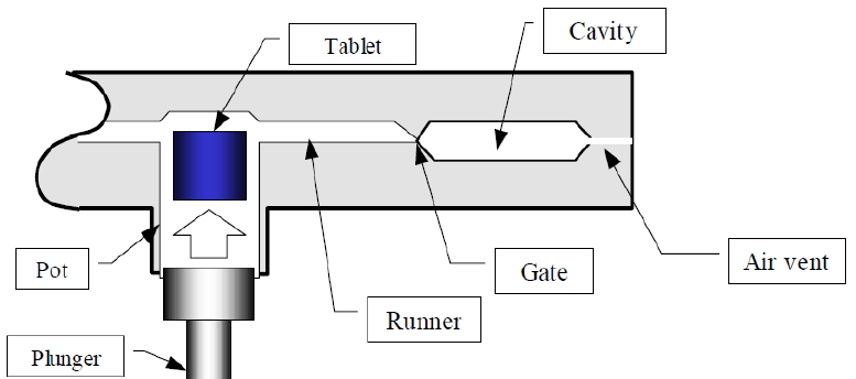
Fig. 1 IC encapsulation process
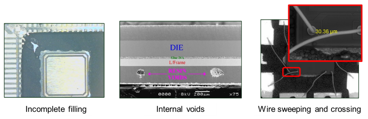
Fig. 2 Common problems in IC packaging
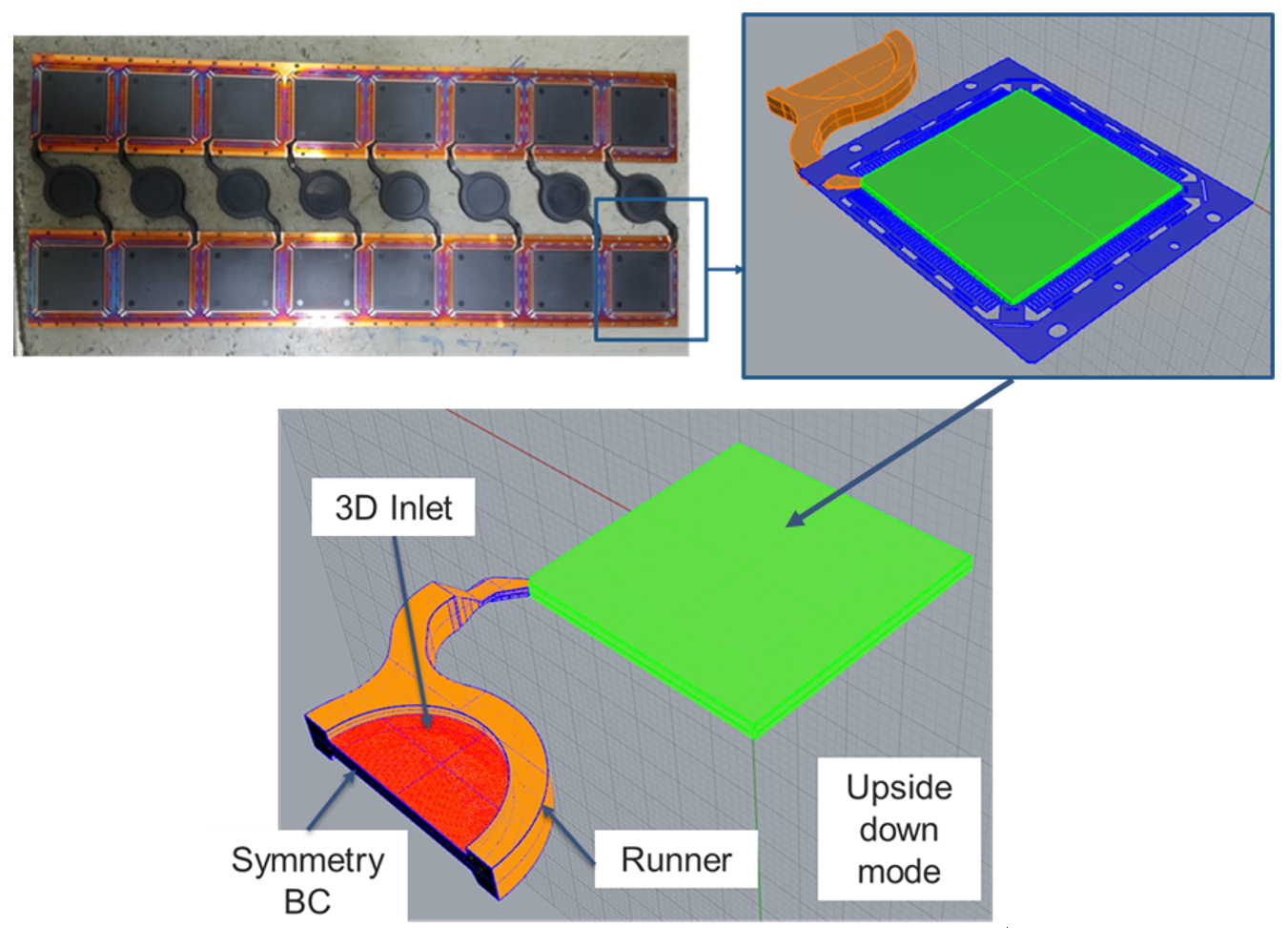
Fig. 3 Real model and mesh built in Moldex3D Mesh
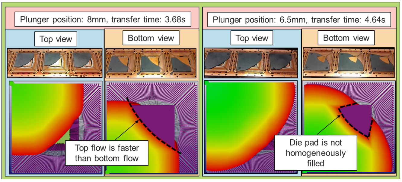
Fig. 4 Experiment vs simulation of the original design
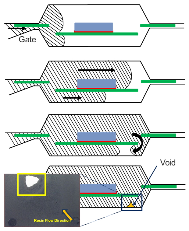
Fig. 5 The melt front behaviors during the filling stage
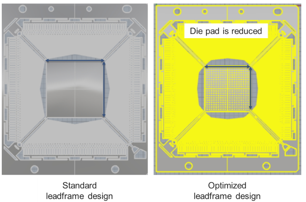
Fig. 6 The lead frame design between original and optimized
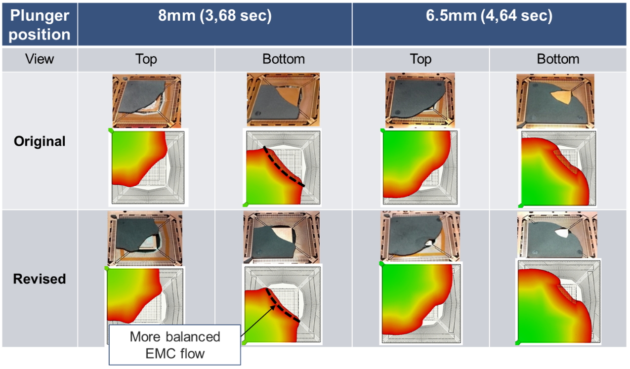
Fig. 7 The melt front of original vs revised designs
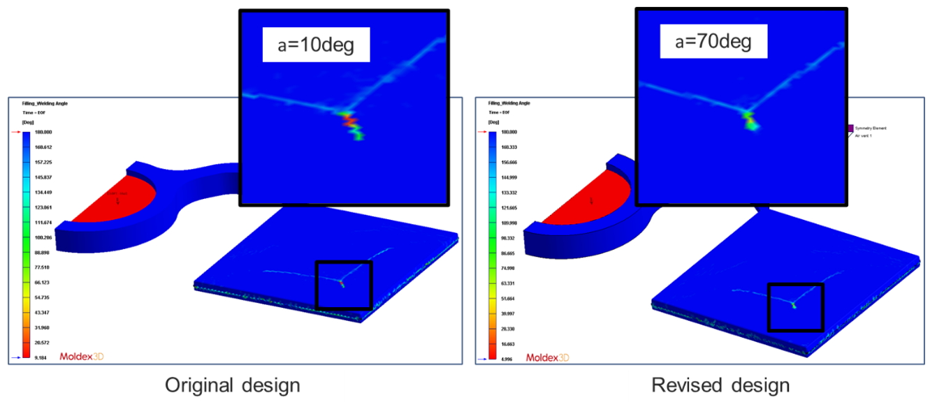
Fig. 8 Weld line results of the original vs revised designs
Results